
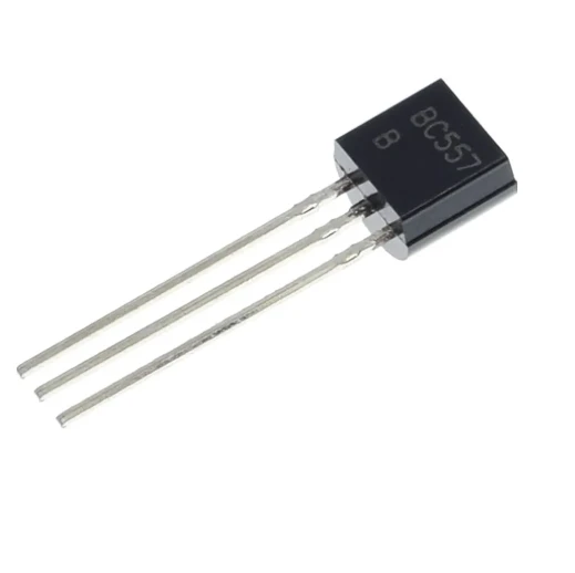
BC557 is
a PNP transistor hence the collector and emitter will be closed
(Forward biased) when the base pin is held at ground and will be opened
(Reverse biased) when a signal is provided to base pin. This is where a PNP
transistor differs from a NPN transistor, a Logic state (blue colour) is used
to toggle between Ground and Signal Voltage (Emitter-Base Voltage VBE) as shown below
BC557 has a gain value of
110 to 800, this value determines the amplification capacity of the transistor.
The maximum amount of current that could flow through the Collector pin is
100mA, hence we cannot connect loads that consume more than 100mA using this
transistor. To bias a transistor, we have to supply current to base pin, this
current (IB) should be limited to 5mA.
When this transistor is
fully biased then it can allow a maximum of 100mA to flow across the collector
and emitter. This stage is called Saturation
Region and the typical voltage allowed across the Collector-Emitter
(VCE) or Base-Emitter (VBE) could be 200
and 900 mV respectively. When base current is removed the transistor becomes
fully off, this stage is called as the Cut-off
Region and the Base Emitter voltage could be around 660 mV.
Features/Specs:
· Bi-Polar PNP Transistor
· DC Current Gain (hFE) is 300 maximum
· Continuous Collector current (IC) is 100mA
· Collector-Emitter Voltage (VCE) is 45V
· Emitter Base Voltage (VBE) is 5V
· Base Current(IB) is 5mA maximum
· Available in To-92 Package
No review given yet!
 Fast Delivery all across the country
 Safe Payment
 7 Days Return Policy
 100% Authentic Products


You need to Sign in to view this feature
This address will be removed from this list


